
Hourly ·
IBM Breaks the 1-Nanometre Barrier with NanoStack Chip Architecture
IBM unveils the world's first sub-1nm chip technology, packing nearly 100 billion transistors onto a fingernail-sized die using a 3D 'block of flats' design.
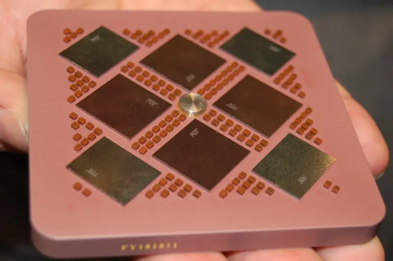
IBM has claimed a historic milestone in semiconductor engineering, unveiling what it describes as the world's first chip technology below 1 nanometre. Dubbed NanoStack, the new architecture crams nearly 100 billion transistors onto a silicon die the size of a fingernail — roughly double the density of IBM's own 2nm test chip demonstrated in 2021.
The breakthrough, announced on June 25 from IBM's Albany research facility, represents the equivalent of a 0.7 nanometre — or 7 angstrom — process node. IBM's internal benchmarking against its 2nm chip showed a 50% performance improvement and 70% greater energy efficiency, along with a 40% improvement in SRAM cell area scaling.
At the heart of NanoStack is a three-dimensional vertical design. Rather than laying transistors side by side, IBM stacks and staggers nanosheet-based transistors along the z-axis. Each transistor uses three sub-5nm-thick nanosheets — roughly 15 silicon atoms across — separated by 9nm spacers. Two such devices are then bonded vertically.
Professor Alan Woodward, a computer scientist at the University of Surrey, compared the approach to urban planning. "IBM's NanoStack is like proposing a 100-storey skyscraper," he told the BBC, adding that rivals Samsung and Intel are closer to "30-50 storey buildings" with their own 3D designs.
Jay Gambetta, Director of IBM Research, called it "a landmark moment" for the chip industry. "We're not just making smaller transistors — we're reinventing how chips are built to deliver dramatically more power and energy efficiency," he said.
The advance comes as the semiconductor industry grapples with the physical limits of Moore's Law. TSMC, Intel, and Samsung have all been targeting low-single-nanometre production within two years, but sub-1nm chips were widely expected to remain out of reach until the end of the decade. IBM's announcement accelerates that timeline — though the company acknowledges commercial production is still years away.
Key to the achievement is advanced lithography. IBM and partners including ASML, Lam Research, Tokyo Electron, and SCREEN are using High-NA EUV (extreme ultraviolet) equipment at the Albany Nanotech Complex to pattern features at angstrom-class scales.
Huiming Bu, IBM's VP of silicon technology R&D, said NanoStack "is a new paradigm" that could give the industry "at least another decade" of scaling headroom. IBM stressed that NanoStack is a generic logic technology expected to eventually underpin CPUs, GPUs, mobile SoCs, and SRAM arrays — with AI and cloud workloads as primary beneficiaries.
"Everyone demands more performance, but no one wants to pay the bill for the power," Bu said. "This new innovation can improve performance by 50% compared to the best available chip today, and at the same time cut energy by 70%."
The challenges are real. Stacking transistors vertically creates heat dissipation problems — hot transistors warm the layers above them — and ultra-thin layers can prevent transistors from switching off properly. IBM said it has experimentally validated solutions including ultra-thin dielectric bonding and dual-channel engineering across the stacked devices.
While commercial viability remains years out, the NanoStack milestone signals that the decades-long race to shrink transistors still has room to run — it's just changing direction, from flat to vertical.
Content on Anagnorisis is summarized, paraphrased, and editorialized from publicly available sources for length and clarity. Original sources are linked where available. All trademarks belong to their respective owners.